Host Memory Buffer: A Smarter Path for PCIe DRAM-less SSDs
Why SSDs Need More Than Just NAND
Just as a computer relies on RAM to temporarily hold the information it's actively working with, an SSD depends on its own form of short-term memory to operate efficiently. Memory buffers, such as DRAM and SRAM, are the SSD’s supercharger, boosting NAND's inherent speed with extra clout for high-speed lookups and data staging for faster access and transfer. To understand why this matters, it’s important to look at what happens during a typical SSD read operation and why modern SSDs depend so heavily on efficient metadata handling.
Before diving into how these buffers work, let’s first understand how an SSD retrieves data.
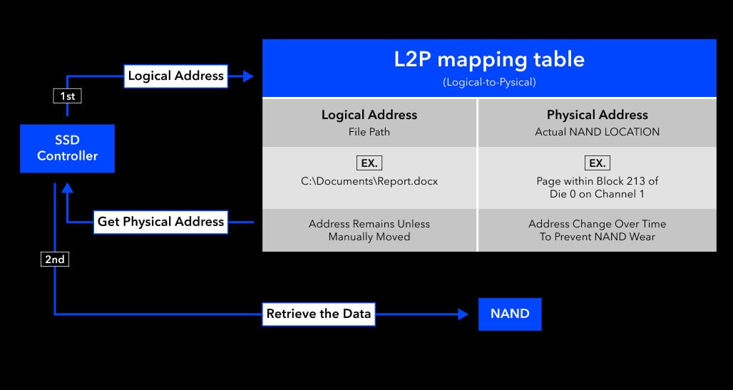
In an SSD, when the system requests to read a piece of data, the SSD controller (the internal processor that manages all drive operations) needs to refer to a mapping table to locate the physical address in NAND Flash that corresponds to the logical address (LBA, Logical Block Address). This mapping table is called the L2P (Logical-to-Physical) table.
- Logical Address:
The location where the host system thinks the data is stored— like a file path you see in Windows (e.g., "C:\Users\Yourname\Documents\whitepaper.docx") - Physical Address:
The actual physical block in NAND where the data is located (e.g., "block 2000")
Once the controller looks up the L2P table and retrieves the corresponding physical address, it can fetch the data directly from the correct NAND block and return it to the host.
However, these physical locations are not static. NAND Flash can only endure a limited number of write cycles on any given block, so SSD controllers frequently relocate data in the background to distribute writes evenly — a process known as wear leveling. This prevents any single block from wearing out prematurely and extends the overall lifespan of the drive.
As a result, the physical location of data is constantly shifting, which is exactly why the L2P table is so critical: it ensures the system always retrieves the correct data regardless of where it has been moved.
Because of this constant remapping, the speed at which the SSD can access and reference the L2P table becomes a major bottleneck, especially in random workloads.
Two Types of SSDs: DRAM-equipped vs. DRAM-less
Not all SSDs handle the L2P table the same way. Depending on the design, an SSD may store and access this critical mapping table very differently — and that difference has a direct impact on performance.
Some SSDs come equipped with a dedicated DRAM buffer, working alongside the controller's built-in SRAM (on-die memory), to store the L2P table and serve as a high-speed cache. Because DRAM operates at significantly higher speeds than NAND Flash, this design allows the controller to look up mapping data almost instantly, reducing lookup latency and improving overall responsiveness.
In DRAM-less SSDs, however, the L2P table resides in NAND itself. This means each read operation may require two separate NAND accesses: one to fetch the mapping, and another to retrieve the actual data, adding overhead that noticeably impacts response times.
This penalty is especially significant during random read workloads. Unlike sequential reads (such as playing a video or loading large files), random read operations access scattered data across the drive. Each read must first look up the L2P mapping, which adds extra steps and affects performance.
Example of random read:
- Booting a computer: the system loads the OS, drivers, and settings, which heavily rely on random read performance.
Furthermore, this repeated back-and-forth increases write amplification, accelerating NAND wear beyond what normal usage would cause. All of these factors highlight why memory buffers are so essential — without them, the SSD is forced to do significantly more work for every single operation.
The Trade-offs of Carrying Your Own Buffer
While DRAM-equipped SSDs deliver optimal performance, they also introduce additional design considerations. Among these, cost and physical footprint become particularly important factors, especially in environments where every dollar and every millimeter counts.
- Cost Efficiency
Integrating dedicated DRAM into an SSD adds to the overall bill of materials (BOM). For applications in embedded, industrial, and edge deployments, where procurement decisions are often driven by strict budget requirements, this additional component cost is a meaningful trade-off to weigh against the performance benefits that DRAM brings.
- Space Considerations
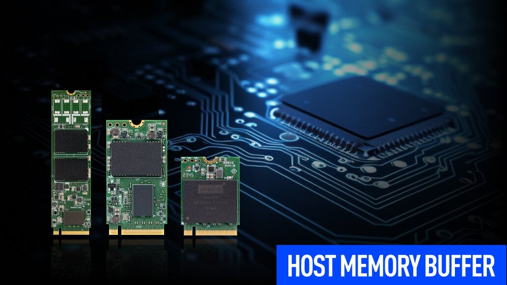
Beyond cost, DRAM chips occupy additional PCB area and require extra routing, which places real constraints on how compact a design can be. In space-constrained environments such as embedded or industrial systems, a DRAM-equipped SSD is not always the most practical fit. Smaller form factors such as M.2 P30 and P42, for instance, simply do not have the physical room to accommodate dedicated DRAM, making a leaner architecture the only viable path for these platforms.
Together, these considerations reflect why storage design is rarely a one-size-fits-all decision. As demand grows for solutions that balance efficiency, footprint, and performance, the NVMe specification introduces an optional feature known as Host Memory Buffer (HMB). This capability enables DRAM-less SSDs to achieve performance levels closer to DRAM-equipped designs without incurring the cost or space overhead of dedicated onboard DRAM.
Host Memory Buffer: Giving PCIe DRAM-less SSDs a Smarter Boost
Host Memory Buffer (HMB) allows a DRAM-less SSD to access a portion of the host system’s memory through the PCIe interface and use it as a buffer for caching critical data structures such as the L2P mapping table. By leveraging host memory in this way, DRAM-less drives can recover a significant portion of the performance traditionally associated with DRAM-equipped models.
In other words, instead of copying the original L2P table from NAND Flash into the SSD’s onboard DRAM buffer, a DRAM-less solution leverages HMB to cache this table, enabling fast lookup and reducing access latency.
HMB is not a physical component but an NVMe protocol feature that requires support from the SSD controller architecture, firmware implementation, and host platform. As a result, not all DRAM-less SSDs support HMB despite the mechanism being defined in the NVMe specification.
While DRAM-equipped SSDs can cache various types of data thanks to their onboard memory, DRAM-less SSDs using HMB focus solely on metadata such as the L2P table. This targeted use keeps host overhead low while still delivering performance levels comparable to the benefits normally provided by DRAM.
How HMB Establishes Shared Memory with the Host
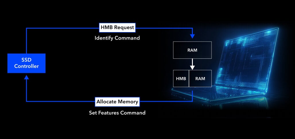
HMB is defined in the NVMe 1.2 spec. Here’s how it operates:
- The SSD notifies the host it supports HMB and requests a specific memory size via the Identify command.
- The host evaluates system RAM availability.
- If resources allow, the host responds using the Set Features command to allocate the memory and provide access details.
Through this handshake, the SSD can now use part of the host's memory as its own cache to speed up operations.
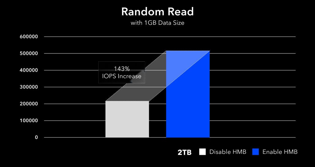
Test data further demonstrates that enabling HMB leads to noticeable improvements in SSD random read speeds. To quantify these gains, we conducted IOMeter benchmarks using a 1GB data size to compare random read performance with HMB enabled versus disabled.
As illustrated in the chart below featuring the Innodisk PCIe Gen4 4TE2 series, the integration of HMB significantly boosts IOPS (Input/Output Operations Per Second). These gains are most evident in random read benchmarks and real-world boot scenarios, where fast L2P access contributes directly to a smoother user experience.
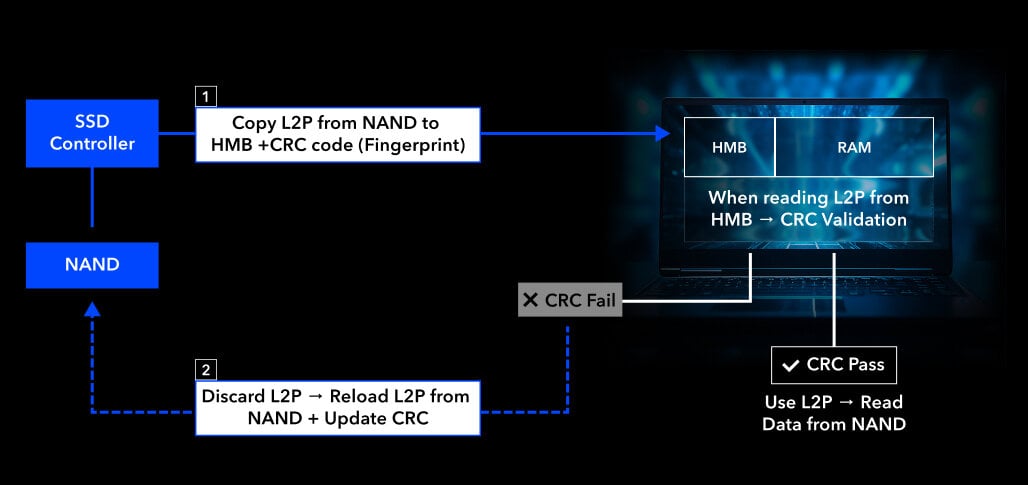
CRC Protection: Ensuring Reliability in HMB-based Designs
Host Memory Buffer (HMB) relies on shared system RAM beyond the SSD’s direct control. To ensure cached data remains accurate—even during system multitasking or potential interference—Cyclic Redundancy Check (CRC) is employed as a data integrity safeguard. CRC plays a critical role in protecting the L2P mapping table while it resides outside the SSD and is transferred between the host and the device, thereby maintaining overall SSD data consistency.
CRC works by generating a short, fixed-length “fingerprint” from the data content. When the SSD writes the L2P table into the HMB, it simultaneously calculates a CRC for that table and stores it in the SSD’s internal SRAM or NAND metadata area.
Later, when retrieving the L2P table from the HMB, the SSD generates a new CRC from the returned table and compares it with the stored one.
- If they match — the table is trusted, and its address mappings are used to locate data in NAND.
- If they don’t match — the table is assumed to be corrupted, discarded, and reloaded from NAND into the HMB with a new CRC.
This verification process ensures that HMB-enabled SSDs maintain reliable performance even in systems with heavy multitasking or limited memory stability. Importantly, this verification adds only minimal overhead, ensuring that reliability is improved without introducing noticeable latency to SSD operations.
Conclusion and Innodisk’s Reliable Solutions
While SSDs with onboard DRAM still offer outstanding performance, HMB-enabled DRAM-less SSDs provide a highly efficient alternative. HMB enables direct interaction between the SSD and host DRAM via PCIe, simulating the behavior of a shared memory system. This design helps DRAM-less SSDs significantly reduce lookup time and improve random read responsiveness.
As more system designers prioritize compact form factors and optimized BOM, HMB’s ability to leverage host memory serves as an elegant bridge between affordability and performance, making DRAM-less SSDs ideal for embedded, industrial, and cost-constrained applications.
Innodisk focuses on comprehensive industrial solutions and has long invested in deep research and development across hardware, firmware, and software technologies. As a result, Innodisk offers a diverse portfolio of storage solutions, including both DRAM-equipped and DRAM-less SSDs to meet different system requirements.
Innodisk’s PCIe storage lineup, which includes the PCIe Gen4 4TE2 & 4TE3 series, and the PCIe Gen3 3TE8 series, supports HMB across the full DRAM-less portfolio. Beyond HMB, these drives incorporate industrial-grade features such as AES 256-bit data encryption and TCG Opal 2.0 support, enhancing reliability and providing secure, durable, and dependable storage that gives embedded and industrial deployments greater peace of mind.

How CXL Breaks the Memory Bottleneck
As AI and real-time processing workloads continue to grow, systems increasingly rely on more powerful CPUs and accelerators to process large amounts of data. As compute capability increases, system architects are hitting the memory wall faster than ever.